LM317 VARIABLE POWER SUPPLY


Original source:

Who knows? Has been around for decades.

Description:

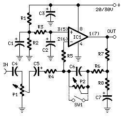
A truly timeless circuit. LM317 is a versatile and highly efficient 1.2-37V voltage regulator that can provide up to 1.5A of current with a large heat sink. It's ideal for just about any application. This was my first workbench power supply and I still use it.

Since LM317 is protected against short-circuit, no fuse is necessary. Thanks to automatic thermal shutdown, it will turn off if heating excessively. All in all, a very powerful (and affordable!) package, indeed.

Although LM317 is capable of delivering up to 37V, the circuit pictured here is limited to 25V for the sake of safety and simplicity. Any higher output voltage would require additional components and a larger heat sink.

Make sure that the input voltage is at least a couple of Volts higher than the desired output. It's ok to use a trimmer if you're building a fixed-voltage supply.

Problems:

Follow all the safety precautions when working with mains voltage. Insulate all connections on the transformer.

Possible uses:

Variable workbench power supply, fixed-voltage supply... Just about any possible application when no more than 1.5A is necessary.


Source: http://www.geocities.com/tomzi.geo/lm317/lm317.htm

High Quality, powerful unit: 90W into 4 Ohm load
Also suited as guitar or bass amplifier


Circuit diagram:
Parts:

R1______________47K 1/4W Resistor

R2_______________4K7 1/4W Resistor
R3______________22K 1/4W Resistor
R4_______________1K 1/4W Resistor
R5,R12,R13_____330R 1/4W Resistors
R6_______________1K5 1/4W Resistor
R7______________15K 1/4W Resistor
R8______________33K 1/4W Resistor
R9_____________150K 1/4W Resistor
R10____________500R 1/2W Trimmer Cermet
R11_____________39R 1/4W Resistor
R14,R15___________R33 2.5W Resistors
R16_____________10R 2.5W Resistor
R17_______________R22 5W Resistor (wirewound)

C1_____________470nF 63V Polyester Capacitor
C2_____________470pF 63V Polystyrene or ceramic Capacitor
C3______________47µF 63V Electrolytic Capacitor
C4,C8,C9,C11___100nF 63V Polyester Capacitors
C5______________10pF 63V Polystyrene or ceramic Capacitor
C6_______________1µF 63V Polyester Capacitor
C7,C10_________100µF 63V Electrolytic Capacitors

D1___________1N4002 100V 1A Diode
D2_____________5mm. Red LED

Q1,Q2,Q4_____MPSA43 200V 500mA NPN Transistors
Q3,Q5________BC546 65V 100mA NPN Transistors
Q6___________MJE340 200V 500mA NPN Transistor
Q7___________MJE350 200V 500mA PNP Transistor
Q8___________IRFP240 200V 20A N-Channel Hexfet Transistor

Q9___________IRFP9240 200V 12A P-Channel Hexfet Transistor


Power supply circuit diagram:

Parts:

1_______________3K9 1W Resistor


C1,C2_________4700µF 63V Electrolytic Capacitors (See Notes)
C3,C4__________100nF 63V Polyester Capacitors

D1_____________400V 8A Diode bridge
D2_____________5mm. Red LED

F1,F2__________4A Fuses with sockets

T1_____________230V or 115V Primary, 30+30V Secondary 160VA Mains transformer

PL1____________Male Mains plug

SW1____________SPST Mains switch


Comments:

To celebrate the hundredth design posted to this website, and to fulfil the requests of many correspondents wanting an amplifier more powerful than the 25W MosFet, a 60 - 90W High Quality power amplifier design is presented here.
Circuit topology is about the same of the above mentioned amplifier, but the extremely rugged IRFP240 and IRFP9240 MosFet devices are used as the output pair, and well renowned high voltage Motorola's transistors are employed in the preceding stages.
The supply rails voltage was kept prudentially at the rather low value of + and - 40V. For those wishing to experiment, the supply rails voltage could be raised to + and - 50V maximum, allowing the amplifier to approach the 100W into 8 Ohm target: enjoy!
A matching, discrete components, Modular Preamplifier design is available here: Modular Audio Preamplifier.

Notes:

In the original circuit, a three-diode string was wired in series to R10. Two of these diodes are now replaced by a red LED in order to achieve improved quiescent current stability over a larger temperature range. Thanks to David Edwards of LedeAudio for this suggestion.
A small, U-shaped heatsink must be fitted to Q6 & Q7.
Q8 & Q9 must be mounted on large heatsinks.
Quiescent current can be measured by means of an Avo-meter wired in series to the positive supply rail and no input signal.
Set the Trimmer R10 to its minimum resistance.
Power-on the amplifier and adjust R10 to read a current drawing of about 120 - 130mA.
Wait about 15 minutes, watch if the current is varying and readjust if necessary.
The value suggested for C1 and C2 in the Power Supply Parts List is the minimum required for a mono amplifier. For optimum performance and in stereo configurations, this value should be increased: 10000µF is a good compromise.
A correct grounding is very important to eliminate hum and ground loops. Connect to the same point the ground sides of R1, R3, C2, C3 and C4 and the ground input wire. Connect R7 and C7 to C11 to output ground. Then connect separately the input and output grounds to the power supply ground.
.

Source: http://www.redcircuits.com/Page100.htm

High Quality simple design No need for a preamplifier


Circuit diagram:

Parts:

R1,R4_________47K 1/4W Resistors

R2____________4K7 1/4W Resistor
R3____________1K5 1/4W Resistor
R5__________390R 1/4W Resistor
R6__________470R 1/4W Resistor
R7___________33K 1/4W Resistor
R8__________150K 1/4W Resistor
R9___________15K 1/4W Resistor
R10__________27R 1/4W Resistor
R11_________500R 1/2W Trimmer Cermet
R12,R13,R16__10R 1/4W Resistors
R14,R15_____220R 1/4W Resistors
R17___________8R2 2W Resistor
R18____________R22 4W Resistor (wirewound)

C1___________470nF 63V Polyester Capacitor
C2___________330pF 63V Polystyrene Capacitor
C3,C5________470µF 63V Electrolytic Capacitors
C4,C6,C8,C11_100nF 63V Polyester Capacitors
C7___________100µF 25V Electrolytic Capacitor
C9____________10pF 63V Polystyrene Capacitor
C10____________1µF 63V Polyester Capacitor

Q1-Q5______BC560C 45V 100mA Low noise High gain PNP Transistors
Q6_________BD140 80V 1.5A PNP Transistor
Q7_________BD139 80V 1.5A NPN Transistor
Q8_________IRF530 100V 14A N-Channel Hexfet Transistor

Q9_________IRF9530 100V 12A P-Channel Hexfet Transistor


Power supply circuit diagram:


Parts:

R1____________3K3 1/2W Resistor


C1___________10nF 1000V Polyester Capacitor
C2,C3______4700µF 50V Electrolytic Capacitors
C4,C5_______100nF 63V Polyester Capacitors

D1__________200V 8A Diode bridge
D2__________5mm. Red LED

F1,F2_______3.15A Fuses with sockets

T1__________220V Primary, 25 + 25V Secondary 120VA Mains transformer

PL1_________Male Mains plug

SW1_________SPST Mains switch


Notes:


Can be directly connected to CD players, tuners and tape recorders. Simply add a 10K Log potentiometer (dual gang for stereo) and a switch to cope with the various sources you need.
Q6 & Q7 must have a small U-shaped heatsink.
Q8 & Q9 must be mounted on heatsink.
Adjust R11 to set quiescent current at 100mA (best measured with an Avo-meter connected in series to Q8 Drain) with no input signal.
A correct grounding is very important to eliminate hum and ground loops. Connect to the same point the ground sides of R1, R4, R9, C3 to C8. Connect C11 to output ground. Then connect separately the input and output grounds to power supply ground.
An earlier prototype of this amplifier was recently inspected and tested again after 15 years of use. Results, comments and pictures are shown here.


Source: http://www.redcircuits.com/Page2.htm

High Quality, simple design 20 to 30V supply


Circuit diagram:


Parts:

P1_________________10K Log.Potentiometer (Dual-gang for stereo)

P2________________100K Log.Potentiometer (Dual-gang for stereo) (See Notes)

R1,R2_____________100K 1/4W Resistors
R3,R6______________15K 1/4W Resistors
R4_________________10K 1/4W Resistor
R5_________________22K 1/4W Resistor
R7__________________1K 1/4W Resistor
R8________________560R 1/4W Resistor

C1,C2,C5____________2µ2 63V Electrolytic Capacitors
C3________________470µF 35V Electrolytic Capacitor
C4__________________1µF 63V Polyester Capacitor
C6_________________47nF 63V Polyester Capacitor
C7_________________22µF 25V Electrolytic Capacitor

IC1_______________TL072 Dual BIFET Op-Amp

SW1________________DPST Switch (Optional, see Notes)


Comments:

This preamplifier was designed to cope with CD players, tuners, tape recorders etc., providing an ac voltage gain of 4, in order to drive less sensitive power amplifiers. As modern Hi-Fi home equipment is frequently fitted with small loudspeaker cabinets, the bass frequency range is rather sacrificed. This circuit features also a bass-boost, in order to overcome this problem. You can use a variable resistor to set the bass-boost from 0 to a maximum of +16dB @ 30Hz. If a fixed, maximum boost value is needed, the variable resistor can be omitted and substituted by a switch.


Notes:

Schematic shows left channel only, but R1, R2, R3 and C1, C2, C3 are common to both channels.
For stereo operation P1, P2 (or SW1), R4, R5, R6, R7, R8 and C4, C5, C6, C7 must be doubled.
Numbers in parentheses show IC1 right channel pin connections.
A log type for P2 ensures a more linear regulation of bass-boost.
Needing a simple boost-in boost-out operation, P2 must be omitted and SW1 added as shown in the diagram.
For stereo operation SW1 must be a DPST type.
Please note that, using SW1, the boost is on when the switch is open, and off when the switch is closed.


Source: http://www.redcircuits.com/Page60.htm


Parts:
R1_____________10K 1/4W Resistor
R2,R5,R6,R9_____1K 1/4W Resistors
R3_____________33R 1/4W Resistor
R4,R8___________1M 1/4W Resistors
R7_____________10K Trimmer Cermet
R10____________22K 1/4W Resistor


C1,C4___________1΅F 63V Electrolytic or Polyester Capacitors
C2_____________47pF 63V Ceramic Capacitor
C3,C5,C6______100΅F 25V Electrolytic Capacitors

D1_____________Infra-red LED
D2_____________Infra-red Photo Diode (see Notes)
D3,D4________1N4148 75V 150mA Diode
D5______________LED (Any color and size)
D6,D7________1N4002 100V 1A Diodes

Q1____________BC327 45V 800mA PNP Transistor

IC1_____________555 Timer IC
IC2___________LM358 Low Power Dual Op-amp
IC3____________7812 12V 1A Positive voltage regulator IC

RL1____________Relay with SPDT 2A @ 220V switch
Coil Voltage 12V. Coil resistance 200-300 Ohm

J1_____________Two ways output socket


Device purpose:

This circuit is useful in liquids level or proximity detection. It operates detecting the distance from the target by reflection of an infra-red beam. It can safely detect the level of a liquid in a tank without any contact with the liquid itself. The device's range can be set from a couple of cm. to about 50 cm. by means of a trimmer.
Range can vary, depending on infra-red transmitting and receiving LEDs used and is mostly affected by the color of the reflecting surface. Black surfaces lower greatly the device's sensitivity.

Circuit operation:

IC1 forms an oscillator driving the infra-red LED by means of 0.8mSec. pulses at 120Hz frequency and about 300mA peak current. D1 & D2 are placed facing the target on the same line, a couple of centimeters apart, on a short breadboard strip. D2 picks-up the infra-red beam generated by D1 and reflected by the surface placed in front of it. The signal is amplified by IC2A and peak detected by D4 & C4. Diode D3, with R5 & R6, compensate for the forward diode drop of D4. A DC voltage proportional to the distance of the reflecting object and D1 & D2 feeds the inverting input of the voltage comparator IC2B. This comparator switches on and off the LED and the optional relay via Q1, comparing its input voltage to the reference voltage at its non-inverting input set by the Trimmer R7.

Notes:

Power supply must be regulated (hence the use of IC3) for precise reference voltages. The circuit can be fed by a commercial wall plug-in power supply, having a DC output voltage in the range 12-24V.

Current drawing: LED off 40mA; LED and Relay on 70mA @ 12V DC supply.

R10, C6, Q1, D6, D7, RL1 and J1 can be omitted if relay operation is not required.

The infra-red Photo Diode D2, should be of the type incorporating an optical sunlight filter: these components appear in black plastic cases. Some of them resemble TO92 transistors: in this case, please note that the sensitive surface is the curved, not the flat one.

Avoid sun or artificial light hitting directly D1 & D2.

Usually D1-D2 optimum distance lies in the range 1.5-3 cm.

If you are needing a similar circuit driving 3 LEDs in sequence, also suitable as a parking aid, click here


Source: http://www.electronics-lab.com


Parts:

U1----------------555 Timer IC

R1----------------47 ohm resistor

R2----------------470 ohm resistor

R3----------------5k variable resistor

C1-----------------0.0047uf ceramic capacitor

LED1,LED2--------Infrared LED's


This circuit oscillates two infrared LED's at 40 khz. To make sure it is transmitting IR light, you can get a little tool from radio shack for about $5. It is a small sheet of plastic about 1" by 3" with a special strip of material, that when exposed to IR light glows (it's actually kinda cool..) A way to check for 40khz IR light is to build a circuit that lights an led when 40khz light is detected. You can get the schematic by clicking here.


Source:http://www.reconnsworld.com


Here is another equally cool low voltage alarm circuit for your glider receiver battery that I've shamelessly stolen from George Steiner's book "A to Z--Radio Control Electronic Journal" (see below). I've modified it to use with small battery packs in R/C gliders. This design has a trigger voltage at about 4.3 volts, and it draws 1mA or less when quiet and about 4mA when buzzing. This can be constructed from parts fromt Radio Shack, though you may need to order a few through them.

The voltage of a receiver system is punctuated by low-voltage spikes every time the servo motors spin up, since the servos draw more than the battery can deliver. With large receiver battery packs, this is not as much of an issue, and it may not be noticeable. However with 270mA and smaller battery packs, particularly with more than two servos, low voltage alarms can chirp constantly, every time a servo moves. The challenge is to design in a little slack or delay, just enough so that you are not annoyed by constant chirping, but not too much so that the chirps can give you a warning before the battery is completely exhausted. Here, this "hysteresis" is adjusted with the capacitor. For large packs (600mA and above), no capacitor is probably needed, although I've been using a 1uF capacitor on my open class ship with 6 servos and a 600mA battery. For 270 mA and two servos, I'd suggest trying a 1uF capacitor. For 150mA or less, a 2.2uF capacitor works well. If you want to know only when the battery has finally reached the trigger voltage, try a 5uF (or 4.7uF) capacitor. The actual type of capacitor is not critical, but tantalum capacitors are physically smaller. If you want to worry about the polarity of the capacitor, the negative side should be directed toward the negative pole of the battery, but at these relatively low voltages compared to the capacitor rating, the polarity probably does not matter.

This circuit is set up for a four cell receiver battery pack at a trigger voltage of about 4.3 volts (about 1.1volts/cell). You can adjust R1 (here a 3.3k resistor) to change the trigger voltage of the circuit. For example, for a 5 cell pack, to change the trigger voltage to 5.5 volts, change R1 to 2.2k. For a three cell pack, to change the trigger voltage to 3.3 volts, change R1 to 6.8 k (or use two 3.3k resistors in parallel by soldering a resistor in each hole and twisting together the top leads). Because of slight variability in tolerances of the componants, you should check this little device with a variable power source and a voltmeter to confirm its trigger point. Alternately, use your digital voltmeter or expanded scale voltmeter to calibrate its chirp pattern by measuring the voltage of the onboard battery pack intermittently as you fly.

Make sure the band on the Zener diode is toward the "+" side (toward R1). Solder a battery connector or servo connector to the board with positive and negative as shown, and plug the connector into an unused slot in your receiver.


Radio Shack parts: Here again, you can use smaller rated resistors if you can get them--1/8 watt or less is fine. Tantalum capacitors are physically smaller, but any composition will work.


Source: http://www.electronics-lab.com


This circuit will allow you to turn on any piece of equipment that operates on 115 volts ac. The reciever circuit is based on the Radio Shack infrared receiver module(MOD), part number 276-137. It is also available from some of the other sources listed on my Links page. The MOD accepts a 40khz IR signal that is modulated at 4 khz. When a signal is recieved the MOD will go low. The sensitivity of the MOD is set by different values for R1 and C1.


The values for R1 may need to be as high as 10,000 ohms and for C1 40uf. This will prevent the unit from turning on under normal lighting conditions. You will need to experiment with the vaules that work best for you. The output of the 4013 chip a flip flop toggles on and off with the reception of a IR pulse. The output of the 4013 turns on the MOC optical coupler which in turn switches on the triac and supplies power to the AC load.


Source: http://www.electronics-lab.com

TX,


This is a 3 channel RF remote control project.The transmitter powered by 3V battery(coin size) range about 10 m. This remote control I use PIC12F509 from Microchip which is a 8-pin single-chip microcontroller designed for low pin count applications with 1 K words flash memory and 41Byte SRAM and some special features such Power-saving Sleep mode,Wake-up from Sleep on pin change.

RX,


Source; http://electronics-diy.com/electronic_schematic.php?id=718

 Schematic: 


Parts:

Part          Total Qty.               Description Substitutions

C1                    1                        0.1uf Ceramic Disc Capacitor 
U1                    1                        DS1669 Digital Pot IC (See Notes) 
S1, S2              2                       Momentary Push Button Switch 
MISC               1                       Board, Wire, Socket For U1


Source: http://www.aaroncake.net/circuits/volume.asp

This is a Li-Po charger and balancer project for R/C hobby.The charger circuit is based on the circuit of Electron head and all folks in the DIY electronics topic on the rcgroups.com.


Detail


U1 do the fucntion constant current with limit curcent by R1 which calculated by

R1 = 1.25/Current in amps of current regulator.

for my project I need to charge 3 cell pack 620mAh.So R1 is

R1 = 1.25/.620 = 2.01612 Ohm

But I don't need to charge at 1C because I'm not sure the actual C rate(actualy may be 98-100% of battery specifications) .In my circuit I need to charge at 600mA or about 96% of 1C and R1 is 2.083 Ohm which formed by 3 X 1 Ohm in series and parallel with 100 Ohm 25 turns trimpot as the above circuit. Then adjust 100 Ohm trimpot to archive 600 mA (measure
by Amp meter at the output of U2)

U2 do the fucntion constant voltage,for 3 cell pack adjust R3 to get the voltage 12.6 v at the output .

Resistor R3(5K) in the balancer section I use 25 turns trimport and adjust to get the accross voltage for each cell is 4.2V (without cell connect).

Warining : Before you build this project please read all the posts in this topics


Source: http://www.coolcircuit.com/project/lipo_charger/lipo_charger.html

This is a NiCd/Ni-MH charger that can charge with constant current and automatic charge termination when the total voltage for all cells reach the setting voltage.

I design this project to charge for 4 cells Ni-Cd/Ni-MH only .After assembly all components into PCB then adjust VR1 to get the voltage at pin 5 of LM555 is 5.8-5.9V or about 1.45 V/cell (1.45 x 4 = 5.8V) 

This circuit charging the battery at about 270 mAh or 10% of C (my battery is sanyo Ni-MH 2700mAh) .You can change the charge current by replace R2.


The charge termination when the voltage at pin 6 of LM555(total cells voltage) reach to the voltage of pin 5 of LM555 and the relay1 turn off so no power consumption when charging complete becuase it open the main AC power supply. This project like a general night chager in the market beause it take a long time to complete charging.


Source: http://www.coolcircuit.com/project/nicd_charger1/nicd_charger.html


This is a small and light weight Battery Eliminator Circuits(BEC).The heart of this project are four very low dropout linear regulator L4941.The DPAK packages to be used in this project.


DPAK packages

L4941 Feature summary
- Low dropout voltage (450mV typ. at 1A)
- Very low quiescent current
- Thermal shutdown
- Short circuit protection
- Reverse polarity protection

Data sheet L4941
The data sheet in pdf format
Because I need 4A output so I use L4941 x 4 connected in parallel on the single layer PCB.If you worry about the heat that dissipated by L4941 you should mount the small heat sink at the top of IC. but increase a litle weight.


PCB for this project 

All PCB are pdf format included posistive,

Source: http://www.coolcircuit.com/project/bec4a/bec_4a.html

negative buttom and overlay.


The CD 4014 is an 8-stage shift register.

The CD 4014 is a CMOS chip.
Minimum supply voltage 6v
Maximum supply voltage 15v
Max current per output 15mA
Maximum speed of operation 5MHz


Circuits built around a CD 4014:


Source: http://www.talkingelectronics.com/ChipDataEbook-1d/ChipDataEBook-1d.html

CD 4013

CD 4013


The CD 4013 is a DUAL FLIP FLOP. 

The CD 4013 is a CMOS chip.
Minimum supply voltage 6v
Maximum supply voltage 15v
Max current per output 15mA
Maximum speed of operation 5MHz


Circuits built around a CD 4013:


Source: http://www.talkingelectronics.com/ChipDataEbook-1d/ChipDataEBook-1d.html

  TRUTH TABLE


The CD 4011 is the most used CMOS chip.

It contains 4 NAND gates.
Minimum supply voltage 3v
Maximum supply voltage 15v
Max current per output 10mA
Maximum speed of operation 4MHz

Current consumption approx 1uA


Follow the inputs and note when the LED is illuminated.


GATING: 
The secret to understanding the operation of
the gate is show in the diagram on the right.
It is called GATING.
When one input is held LOW, the output is a constant HIGH.
When one input is held HIGH, the signal on the other input will be inverted by the gate and appear on the output.
This is also shown in the 1kHz tone circuit below.

Note:
Do not leave an input "open" (non-connected) as the high input impedance (approx 10M) will pick up noise and create faulty operation.


The CD 4011 IC has 4 gates and these can be wired to create a BUFFER, Inverter (NOT), AND, OR, NOR XOR or XNOR. In most cases this will use 3 or 4 of the gates and represents a wasteful use of the chip. These examples are useful for demonstration purposes:


Circuits built around a CD 4011:


Source: http://www.talkingelectronics.com/ChipDataEbook-1d/ChipDataEBook-1d.html

TRUTH TABLE


The CD 4001 is a very versatile CMOS chip. It contains 4 NOR gates. Minimum supply voltage 3vMaximum supply voltage 15vMax current per output 10mAMaximum speed of operation 4MHzCurrent consumption approx 1uA


Follow the inputs and note when the LED is illuminated.


GATING:

The secret to understanding the operation of
the gate is show in the diagram on the right.
It is called GATING.
When one input is held LOW, the signal on the other input will be inverted by the gate and appear on the output.
When one input is held HIGH, the output is a constant LOW.
This is also shown in the 1kHz tone circuit below.

Note:
Do not leave an input "open" (non-connected) as the high input impedance (approx 10M) will pick up noise and create faulty operation.


Circuits built around a CD 4001:


Source: http://www.talkingelectronics.com/ChipDataEbook-1d/ChipDataEBook-1d.html

The signal from the transmitter is picked up by the receiver as bursts of tone between hash. Viewing the signal on a CRO (Cathode Ray Oscilloscope) will look something like fig: 23.


                                           The signal from the multi-channel transmitter will consist
                                                    of a regular waveform between background hash.

The receiver is required to pick out the signal from the noise and it does this by a process called integration and differentiation where the signal is detected due to its regular nature and this is used to charge a capacitor. 
Another circuit determines the length of time the tone is present and these are combined to determine the nature of the control signal. Most of the circuitry for doing this is locked inside the chip in the receiver and the only components we can see are the external items on pins 10, 1 and 19. These determine the frequency detected by the chip and the length of the "highs," but all the rest of the signal processing is done inside the chip. The chip detects the waveforms shown in figs 14 - 19 and turns on the appropriate outputs.

                                              A multi-channel 2MHz receiver

                                                The 27MHz receiver PC board

Two outputs drive the motor in the forward/reverse direction and 4 outputs drive the transistors for the steering motor. The steering motor is simply a rotary actuator. This is similar to the armature of a motor, positioned inside a circular magnet.
The armature does not need brushes as it will only turn about 45° in one direction and 45° in the opposite direction, depending on the direction of the current. The output of the shaft will be connected to a lever to steer the front wheels.
The chip controls the two diagonally opposite transistors for the clockwise and anticlockwise rotation to get left and right steering. All the rest of the circuit has been previously discussed and the only new feature is the tapping at 4.5v for the motor. A diode on the 4.5v rail drops the voltage to 3.8v and the two output transistors drop a further 1v, so that motor receives about 2.8 to 3v.

Here are some remote control items, shown on the web, by a hobbyist who disassembles devices and makes a new project:

Some of these components were used to build a project and presented on the web.


Source: http://talkingelectronics.com

The second receiver circuit we will study uses more components to do exactly the same job but it may have better sensitivity due to the inclusion of one extra stage of amplification and the use of a higher rail voltage. The higher rail voltage gives some stages a higher gain due to the higher amplitude of the signal. But some of the gain has been lost in the diode pump as this type of pump requires more energy to charge the 10u than a 0.47u. The use of a center-tapped voltage source saves two transistors in the bridge network but necessitates the use of a double-pole switch to disconnect both halves of the supply.

                                          A 27MHz receiver using a split supply 
                                                     The 27MHz receiver PC board


Source: http://talkingelectronics.com

This circuit uses the TX-2B RX-2B chipset discussed on the previous page. The chip has 5 channels and the circuit uses 4.
Click HERE for TX-2B RX-2B chipset datasheet .pdf


                                             4-Channel Transmitter PC Board

                                                       TX-2B circuit on datasheet


The receiver using the RX-2 chip:


                                                     4-Channel Receiver PC Board


                                                  RX-2B circuit on datasheet

Source: http://talkingelectronics.com

MediaEXL

MediaEXL Hit Counter

Join 4Shared Now!

Hit Counter

Find more freelance jobs